Qualcomm recently launched its flagship Snapdragon 8 Elite Gen 5 chipset, which uses TSMC’s 3nm process.
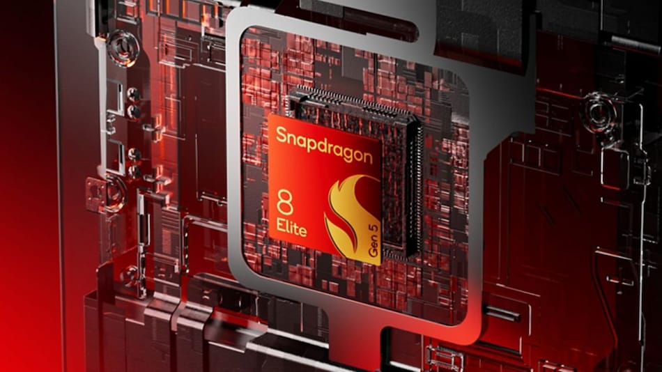
Snapdragon 8 Elite Gen 5 chip was internally codenamed SM8850
Click Here to Add Gadgets360 As A Trusted Source

Qualcomm’s next-generation Snapdragon 8 Elite Gen 6 chip is expected to launch next year during the firm’s annual Snapdragon Summit. The chipmaker recently unveiled the Snapdragon 8 Elite Gen 5, which powers recently unveiled flagship phones like the OnePlus 15, iQOO 15, Realme GT 8 Pro, Red Magic 11 Pro, Nubia Z80 Ultra, and the Xiaomi 17 lineup. This year’s chipset is built on a 3nm process technology and supports LPDDR5x RAM. A tipster now claims that the purported Snapdragon 8 Gen 6, will be fabricated using TSMC’s 2nm process technology and supports LPDDR6 RAM and UFS 5.0 storage.
Snapdragon 8 Elite Gen 6 Tipped to Increase Cost of Flagship Phones
In a post on Weibo, tipster Digital Chat Station (translated from Chinese) leaked key details about the rumoured Snapdragon 8 Elite Gen 6 chipset. The user, who has a good track record of leaking mobile-related information, believes that the chip will be produced using TSMC’s 2nm N2P process technology and phones equipped with these chips could be more expensive than their predecessors. The phones powered by the purported chip might support LPDDR6 RAM and UFS 5.0 onboard storage.
Moreover, Qualcomm’s N2P-based Snapdragon 8 Gen 6 chipset is tipped to offer improved power efficiency and performance compared to the N2 technology. The tipster recently claimed that the chipset has been codenamed SM8975, succeeding the recently launched Snapdragon 8 Elite Gen 5, which is internally referred to as SM8850.
This year’s flagships, like the OnePlus 15, Realme GT 8 Pro, and iQOO 15 are powered by the flagship 3nm chip. Similarly, it is safe to assume that the purported Snapdragon 8 Elite Gen 6 chip will debut on next year’s flagship handsets.


According to TSMC, the N2P technology provides a 5 percent performance improvement over chips made on the company’s current process. It maintains the same architecture rules as the N2 technology, while accounting for “the majority of N2 adoptions”. Additionally, N2P is claimed to deliver 18 percent faster speeds while consuming the same amount of energy and 36 percent enhanced efficiency at the same speed as the N2 with a 2nm node.
Additionally, the chipmaker claims that the N2P technology offers 1.2 times logic density and 1.15 times chip density over the 3nm N3E process. N2X features two elements, including the “ultra-high performance” standard cell and a “high-speed” device to provide a combined faster speed of 10 percent. We can expect to learn more about chips produced using the N2P process in the coming months.